Leakage voltage issue in flyback smps

falcosms

New member
Hello all..

i´m working in a smps flyback 138W DCM


input: 80 - 250 Vac, output 13,8V x 10 A.

the schematic is this: SMPS.jpg
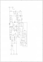
it´s working, but when i apply load (about 4 A) the leakage voltage across the mosfet is very high... look: View attachment osc.bmp.

the transformer is 42/15 core, prim 11 + 11 turns, secondary 3 turns, inductance primary of 150 uH. the assembly of primary and secondary are good.

i´m reading about this issue at web, but i don´t found nothing to solve this.

i think the problem is in the transformer, but i can´t solve.

sincerely

marcelo
 

Attachments

  • SMPS.pdf
    20.1 KB · Views: 73

KX36

New member
That's a normal waveform for a DCM flyback converter's MOSFET drain. The only thing unusual about it is that the duty cycle is quite low, and the power level you want is a bit too high for a DCM topology.

The 350V leading spike is from the transformer's leakage inductance, the 250V plateau is from the input voltage plus the reflected secondary voltage through the turns ratio and the ringing is from the discontinous conduction of the flyback transformer. It rings around the input voltage, which looks to be around 180V.

You can never get rid of leakage inductance completely. The solution is either a soft voltage clamp in the form of an RCD network which you already have as D19/R61/C41 or a hard voltage clamp in the form of a TVS diode in the place of the RCD network. Set the clamp voltage somewhere above the 250V plateau voltage at maximum input voltage. If you removed the RCD clamp, you might see maybe a 500-600V spike instead of the 350V one you have. Maybe the RCD clamp could be tweaked to clamp to a lower voltage if this causes you problems at higher input voltages.

Also I note that you have made quite a typical mistake in that you've added loop compensation at the TL431 error amplifier and again at the UC3845. It's unnecessary. Compensate at the TL431, tie off the VFB pin of the IC to whichever rail causes its error amplifier's output transistor to be in cut-off (For this IC, the error amp output is open collector, so ground the VFB pin) and put the feedback signal from the optocoupler to the COMP pin. Other than that your schematic looks quite good assuming you've correctly calculated the compensation.
 
Last edited:

falcosms

New member
hello

thanks for the replay

That's a normal waveform for a DCM flyback converter's MOSFET drain. The only thing unusual about it is that the duty cycle is quite low

does this low duty cycle affect the waveform??


Also I note that you have made quite a typical mistake in that you've added loop compensation at the TL431 error amplifier and again at the UC3845. It's unnecessary. Compensate at the TL431, tie off the VFB pin of the IC to whichever rail causes its error amplifier's output transistor to be in cut-off (For this IC, the error amp output is open collector, so ground the VFB pin) and put the feedback signal from the optocoupler to the COMP pin. Other than that your schematic looks quite good assuming you've correctly calculated the compensation.

ok, i understand this tip!
 

KX36

New member
The low duty cycle (the time the drain voltage is low vs the entire cycle time in case anyone was wondering, what with the 3 different time segments of the waveform) isn't likely to be a big problem. You can see that the time the flyback transformer is ringing and no energy is being transferred is relatively long so for a given packet of energy across the transformer the peak currents would be higher. This duty cycle would be even lower at high input voltage, but really it's set by the worst case conditions that would make it highest - minimal input voltage and maximum load current. If you want it to be DCM, you have to design for it to stay DCM in these conditions and accept that D will be much lower in the opposite conditions.
 

KX36

New member
Also I note that you have made quite a typical mistake in that you've added loop compensation at the TL431 error amplifier and again at the UC3845. It's unnecessary. Compensate at the TL431, tie off the VFB pin of the IC to whichever rail causes its error amplifier's output transistor to be in cut-off (For this IC, the error amp output is open collector, so ground the VFB pin) and put the feedback signal from the optocoupler to the COMP pin. Other than that your schematic looks quite good assuming you've correctly calculated the compensation.

Note also that if you make this change, the phototransistor will be wired common emitter instead of common collector for this particular IC as you no longer have the inverting stage of the IC's error amplifier and you may want to bias the phototransistor with a higher current to increase its bandwidth. At the moment R60 being 47k biases the transistor with around 100uA. Really you want about 1mA on the transistor which puts maybe 3.5mA on the LED (assuming CTR at LED current of 10mA is the datasheet typical value of 0.5, you have to look at the 4N25 datasheet's normalised CTR to derate the CTR for LED current and that derating looks to be roughly 0.55 at this current, so effective CTR would be around 0.275 although if you start with the CTRmin value it will be less), so reduce R60 to maybe 4k7, put it above the collector rather than below the emitter, reduce R49 to account for the difference and work through the type II compensation example here: http://www.onsemi.com/pub/Collateral/TND381-D.PDF The CNY17 datasheet shows the optocoupler pole frequency increasing vs bias current. The 4N25 datasheet doesn't seem to have this chart so you'd have to work it out with the part in hand as the On Semi link describes.
 
Last edited:

falcosms

New member
hello

in these days, i have had problems with the spikes of leakage inductance....

my transformer is a EE 42/21/15 gapped to 150 uH and i made many assemblies tests (half primary, secundary, other half primary), i tried to make a good assembly between primary and secondary, i try to change the snubber with many values of R and C, but i dont have sucess...

i´m starting to suspect of my lay-out..... i compared my project with a smps 100W from china, but the control IC is another and the inductance of transformer is very differente (450 uH).
 
Top