Sg3525 low power psu for dac

Pichou

New member
Hi Alls !
I'm freshly registered here, but I read you since many years.

Now is my day to take the plunge and to show you my smps project.
I don't have engineer knowledge, only school memories.
Since the time I read the forum trying to understand the smps rules, I have now finished the schematics of a low power switchmode psu for preamp use.

The PSU is based on the SG3525 chip and don't use regulation since I will use some regulators at the outputs.
Push-pull design with TN23/3C90 core transformer with 3 secondary (2 for analog +/GND/- and another for digital +/GND) 2x5 PRIM / 2x9+1x5 turns SEC
I use a mosfet driver TC427 with 2x IRFS7440 MOSFET.
I'm planning to use at maximum SMD components for compact design and because I prefer soldering SMD than through hole (my eyes are still good for the moment :D)
For sure some parts cannot be put in SMD (snubbers essentially).

In attache the schematic of the entire PSU.
Many "sub-block" are inspired from well-know others PSU like BCAE1 or Elliot Sound or valveaudio. I'm not able to design entirely this circuit. So maybe I have done some beginners mitakes.

I will have some questions if someone can look the schematic.
Since the secondary winding ( 8- 9 for digital ) is isolated from the analog windings (4 - 5 - 6 -7), I have 2 dif GND, one digital and one analog. It is good for the DAC.
With this configuration does I need to use 2 common mode inductor (one for each output) or does I need to wind all of the secondary in the same inductor ? If I do thos does I need to connect absolutely the 2 gnd ?
I prefer to use 2 different inductor since for this power, I can probably buy them ready to use.
Since the PSU is unregulated, does I really need the inductors ? I need the cleanest possible psu, and in my head, running unregulated is better for noise.

Any comments or suggestion will be appreciated,

Thanks in advance to those who take time to read the post,

Cheers,View attachment PSU Pichou v3.pdf
 

Pichou

New member
Sorry, missing the parts numbers on the schematics.
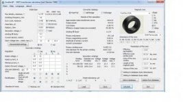
I'm playing with Excellent IT, and I think the TN23 core I planned to use is not good. A TN26 will be better.
Print screen in attache.

IT core psu v3.jpg

View attachment 6459
 

Attachments

  • PSU Pichou v3.pdf
    79.1 KB · Views: 91
Last edited:

Pichou

New member
Hi,
Thanks for your answer :)

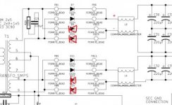
Ouuuupsss 4 diodes in my nose :ambivalence:

I will start routing the board first and I will show you the result.
 

Silvio

Well-known member
@Pichou
Through my experience so far common mode inductors on the output tend to be more noisy than single bead inductors. I do not know what load you have on the output but as the smps is unregulated then noise is not so prominent.
You have enough capacitance on the output to filter out. I also suggest that you make a smaller capacitor such as 1uf film cap instead of the 100uf in the input of the regulators this will filter better any residual noise. You can also try ring inductors but separately wound and not in common mode fashion.

Your input and output snubbers have to be trimmed on the actual setup as ringing if any has to be suppressed on the actual ringing frequency. This tend to vary with different transformers and winding technique.

Use tight coupling and symmetry in your windings to eliminate leakage inductance as much as possible.

Regards Silvio
 

Pichou

New member
Silvio :cool:
Thanks for your answer and advices.
Load on the output will be approx 0.5A on analog symmetric output and something like 1A on digital.

Ok for the capacitors and the inductors. To be sure about the inductors you advise me to use, you talk about one single ring inductor for each transformer output ? Or a common mode for analog and a separate single for digital ?
I have an old amp at home to make some tests (Esoteric 7056, the amp side is burnt put the psu is ok). If i remove the regulation to go 50% duty and the secondary common mode inductor I experiment some ripple. If I leave the inductor in place but still without the regulation, ripple is better.
Something like this can be used for digital side (rated at twice the current needed) ? https://www.mouser.fr/ProductDetail...EpiMZZMsg%2by3WlYCkU%2bb/p1ujdgwWzfYJDYvjIr8=

The snubbers in the schematics are "just to put a value". I will try use this jig to found the correct value when the transformers will work : http://www.diyaudio.com/forums/powe...sformer-snubber-using-quasimodo-test-jig.html
Good idea ?
Anyway, I will leave a place free in the board and populate this only when I will found the good value.

Another question, is, what about the manner I have plug the IN-/IN+/COMP/VREF to run unregulated, do you think it is correct ?

Cheers !
 

Silvio

Well-known member
@Pichou
About the output inductors I was talking about the dual rail output. I was experimenting with smps of higher current than that you are using (8-10A) when I encountered this problem with noise using the common mode inductor wound on the same core for the 2 rails. I got rid of it when I used separate inductor for each rail.

Usually they use a common inductor for several outputs ( Like the ones used in ATX power supplies) These all have a single rail though and not a double output. They do it like this usually for economy and also to get better regulation across all outputs these using the same ferrite ring with separate windings for each rail.
The inductor helps in both ways as it chokes a little the output and also help with better smoothing. It also causes some voltage drop so some headroom in the output for regulation is needed. It will also help out for surges in the output and limits the surge current.


Regarding snubbers well you can also check the blog post I posted called Calculation of snubber components and driver gate resistors.

About the IN+ and IN- I guess you are talking of the sg3525 chip. All I can see is that R15 is too low and this should be around 470K the duty cycle will suffer if it is too low. I also recommend that you make a small preset of around 500R instead of the discharge resistor R9 and then you can set the dead time to around 1-1.5uS. You can put a fixed resistor instead when the correct value is found.

I hope that helps Silvio
 

Pichou

New member
That helps :cool:

Ok for the inductors !
That I can do is to put some dual footprint on the pcb to run common mode or separate inductors (with some headroom between them, I think is necessary) depending results...

I will look your entry blog about snubbers !

Thanks for the correction about the sg3525. I will put 500R for R9 in the schematics and move the value after some tests. I think I need first to have a good square wave signal before moving deadtime (would be difficult to measure DT if the signal have some spikes or other distorded form), so first I will found the good snubbers.

Now, i'm in the routing !
 

Pichou

New member
Hi !
The PSU seems to work properly !
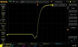
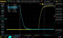
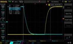
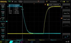
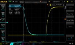
I have play with the snubbers, but i think I don't need them, at the primary and secondary side, there is no overshoot or something strange, it's even the opposite. In attache a view of the mosfet command. Smooth square signal and little undershoot at the end of the waveform.

Silvio, I have try to use your method to found the correct value for the gate resistor, I found 16R. I still use the smallest resistors I have for the moment, 22R....I don't understand the second part of your how to. :(

NewFile2.jpg

NewFile3.jpg
 

Silvio

Well-known member
I was just wondering why you did use the sg3525 for a non regulated power supply for low power. You could have readily used the IR2153. This would have made your circuit easier and having the oscillator and mosfet drive in one package. This chip could handle medium power fets such as IRF840 or IRF740 and a power between 100 and 400 watts can be achieved quite easily.

Regarding the gate resistor, well this calculation allows one to find the correct value for the gate resistor.
This is a combination according to the mosfet driver drive and source current capabilities. The gate resistor is chosen so that the maximum current of the mosfet driver are not exceeded. Hence the mosfet is charged and discharged quickly enough according to the frequency of operation.

Lets consider an IR2153 chip which have a drive and source current of around 200mA and an IR2110 which has a drive and source current of 2A. As one can see the both chips have different current capabilities and the selection of the gate resistor for both chips will be different.
I admit the IR2110 is designed to handle larger mosfets with higher gate charge requirements. The explanation is made so that one can calculate the gate resistor according to the driver used.

It is also important that one must observe the data sheets for both driver and mosfets used. These tend to vary between different manufacturers.

I hope that helps

Regards Silvio
 
Last edited:

Pichou

New member
Silvio, because I have many sg3525 chip in stock bought at very low price. The idea is to start with this small psu, unregulated, and to continue to learn about smps with some sort of regulation and with bigger psu. One chip to learn is enough for me. Maybe it is not the easiest, but for future use I think it's a good choice. I'm not feel good for the moment with alls the different specifications of this sort of chip but I will look the IR2153 for my knowledge.
For the moment the psu works very good on alls the outputs. I can use twice the current I need on outputs without any heat for a total of 3.5A at primary side. Idle current is 0.15A. With my dsp/dac plugged, I draw a total of 1.7A on primary side.
I will try to mount a second psu with just the needed components for the SG to experiment with gate resistor/freq/snubbers/transformer. Maybe I can correct the waveform for a more neat square. The issue seems to be an over-damped form (correct terms ?). I know snubbers can correct overshoot, but here I need the opposite. Right ?
 

Silvio

Well-known member
I don't know where are you measuring that wave form is it from the gates of the mosfets or is it from the output of the SG chip?
It seems that you have a slow rise time and also a slow turn off time. The curves on the wave form clearly shows that. What seems to be the under shoot is the slow turn off and the dead time.
 

Pichou

New member
Hi,

Thanks for your answer Silvio.
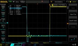
I have done some tests and play with CT/RT/RD to obtain a 1µS dead time and the cleanest square signal I can with just the SG and driver. Ct is 1nF, RT is 15K, RD is 470R. The freq is around 47.5Khz. If I go lower for RD with 250R, dead time is 860ns. With the old CT and RT value charge and discharge time are longer.
I have done some screenshots of the results, hope they are goods for comprehension:
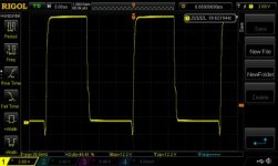
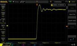
SG3525 output alone, the 2 outputs are identical :
NewFile1.jpg

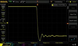
Close view of start and end of the waveform :
NewFile2.jpg
NewFile3.jpg

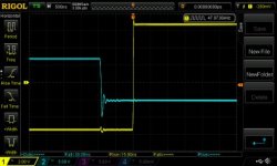
SG3525 + driver TC427 :
NewFile5.jpg


Close view of start and end of the waveform :
NewFile4.jpg
NewFile6.jpg

A view of the 2 waveforms with some markers showing 944ns dead time :
NewFile8.jpg

I can see some ringing in the outputs. What can be the cause ? Routing of the board ?
NewFile7.jpg
 

Silvio

Well-known member
Hello Pichou,

The output from the mosfet driver is most important as this is driving your fets. From what I can see I understand that you have a very nice square wave form coming out to the gates.

Regarding the ringing well this may be caused:-

long runs from driver to gate or from SG to driver.

long leads from driver to mosfet these need to be as short and as thick as possible

High current traces near signal traces thus coupling with them

lastly transformer primary kicks back when switched off from the mosfet. This is only suppressed by a proper snubber across the winding.

usually this ringing is observed only when smps is loaded. The more load the more it rings

One other thing that might be causing ringing is the output inductor. This I have experienced myself and may be the case that you have to make another snubber just after the secondary to suppress any feedback to the trafo

Here is link with some helpful tips for building car audio power supplies

http://www.bcae1.com/switchingpowersupplydesign/switchingpowersupplytut01.htm

Hope that helps
 
Last edited:

Pichou

New member
Your comments are every time useful and welcome ! Thanks for your time !

On the screenshots, there is only the primary side mounted on the board. So ringing is certainly due to my board layout. I think is due to the poor Rigol quality probes too. If I move them vertically to the pcb, ringing is....different...

I will continue to experiment first by calculate and placing gate resistors and mosfets and play with that, make new screenshots and wind a new transformer. When the transformer will be ok, I will continue with new screenshots and by placing rectification and see what happens with a load, add the caps and output inductor etc etc. Step by step approach to learn.

I have a question, does I need to load each output of the transformer to define the primary snubber ? If I understand, this snubber correct only the winding of the primary ? But can pass some strange effects from the secondary like a mirror.
I can put snubbers on secondary side, I have let the place. I can put a snubbers for each secondary output. But for the symmetric analog output, does the best way is to put the snubbers across the 2 legs of the secondary or between each leg and middle point ?

Thanks for the bcae1 link ! I know it and more I read it more I understand the "rules" for smps.
 

Pichou

New member
Some new screenshot of the gate signal direct with the probe on the pin of the mosfet.
I think I have a good (the best) result without gate resistor. A little better slope if I put a 10K in pulldown. I have done some test still without gate resistor but with different value of the pull-down, and if I decrease the value I have very little dead time added and no visible enhancement on the slope of the curve. Does it's a problem to run without gate or pull-down resistor ?

Gate without anything :
NewFile9.jpg

Gate with 10K pull-down :
NewFile10.jpg

Gate with 3K pull-down :
NewFile13.jpg

Gate with 1K pull-down :
NewFile14.jpg
 

Silvio

Well-known member
Hi Pichou,

It is advisable that you use a gate resistor. This will limit the gate current as your diver might not last long without it.
Your driver can deliver around 1.5 amps.

You can take a look at the blog post regarding this subject.If you are using the same fets described in the schematic you posted earlier then use the specified one (22R) You can use a reverse diode to enhance switch off of the fet (1n4148 diode will do) see diagram I posted

The pull down resistor is there to prevent false switching of the fet. The driver actually switches off the fet, 10K ohms is enough in this case.

You can take some scope shots across the primary windings. You will notice that the rise and fall times will be much better there.

.I would like to see some pics of your project this will help me with better suggestions

IMG_0989[1].JPG


regards Silvio
 

Silvio

Well-known member
Regarding the snubber you will try first without it and see how things perform.

If you will be needing to load the smps it does not really matter which winding you load on the secondary it still has the same effect as long as your loads are resistive. (Car bulbs in series will do) I don't know your output voltage/s.

Lastly use symmetry in your windings and tight coupling especially with the main secondary winding which will carry most of the load.
A good transformer is the key for a clean waveform.
 

Pichou

New member
Hi,
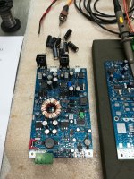
Here is a photo of the psu. Don't know if you can see it in large dimensions...
IMG_20180314_155511.jpg
Transfo is a PRIM 6+6T made with 0.7x1 / SEC1 11+11T with 0.5x1 / SEC2 7T with 0.6x1
RD 470R / CT 1nf / RT 15k / F=48khz
R gate 11R + pull down 10K + Diode like your schematic.
Fall and rise time are better !
Snubber for PRIM is 100nF / 100R. Can't get lower for the resistor or higher for the cap because resistors heat quite a lot...Calculated value is near then 12R....impossible to put that value without huge current consumption and heat...Have to work on this more I think I don't understand or I made mistake somewhere....
No snubber for secondary for the moment.
Iddle current is 0.54A
Secondary voltage with no load at the regulators inputs are : 13.87v for bridge secondary, and +/-22.2v for dual rail output.

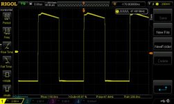
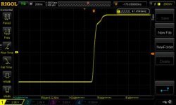
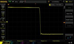
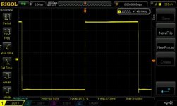
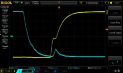
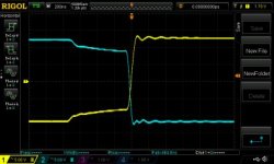
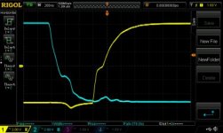
With no load here is some screenshots, strange spike, not seen before....::SD
Gate with no load :
NewFile2.jpgNewFile1.jpg
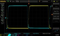
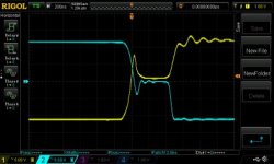
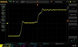
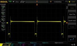
Transformer primary with no load. What cause this "step" ?
NewFile3.jpgNewFile4.jpg
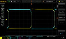
Now some screenshots with load on the output (after the regulators).
1.35A at 7.8V on Digi output, 0.55Ax2 at 12v on analog output, total current drained on primary is 2.52A.
NewFile7.jpgNewFile8.jpg
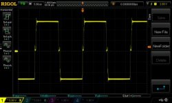
Gate is ok I think, but at the primary of the transformer the "step" is clearly visible. Does it's a problem to have this waveform ?
Because I found the same strange form on secondary....for sure...
Here is a view of the bridge secondary : same "step"
NewFile9.jpgNewFile10.jpg
And a view just after the diodes. This problem is visible even after the diode.NewFile11.jpg
The same problem is visible on the analog dual rail output.
I know I have some parasitics on the gate trace, but all my problems seems to show a bad transformer construction I think...
 
Top