0~500V SMPS based on SG3525

phaedrus

Member
Hi ,

I am designing a 0~500V(25mA) power supply based on the SG3525.The input is a 12V battery.
The transformer was designed using the software available from Vladimir Denisenko, available on this site.
The problem I am facing is that I am getting no output from 0~100V (0~0.5V setting) and then it maxes out at 400V.
I checked the voltage at the set point,it varies from 0~2.5 as per the pot. setting.The voltage at the feedback point also varies as per expectation from 100~400V.
Can anyone suggest any check points on why there is no output from 0 ~ 100v ?
I could probably adjust my turns ratio to get the 500V max. , but i do not know why there is not output voltage from 0~100V.
schematic has been attached FYI.
 

Attachments

  • 0~500V.JPG
    0~500V.JPG
    65 KB · Views: 485

wally7856

New member
I think you should follow the wave form from the sg3525 to the gates, then primary, and then secondary to see if the duty cycle is changing smoothly with your pot.
 

phaedrus

Member
Hi,
Thank you for replying.
At higher values >100V,the duty cycle is very less ( < 5%),but when i go below 100V setting there are no pulses coming to the gate at all.Is it because I am not using a gate driver ?
I am planning to put a TC427 between SG3525 and the IRF540 and check if there is any effect.
Please do chime in with any other suggestions.
 

wally7856

New member
Find a way to remove the wire to the gates of the FET’s or to remove the fet’s. Then check the waveform coming out of the 3525.
 

wally7856

New member
Find a way to remove the wire to the gates of the FET’s or to remove the fet’s. Then check the waveform coming out of the 3525.
 

phaedrus

Member
Hi,
I tried that.The 3525 releases a square wave but only after the set voltage @ pin2 crosses 0.5V.Since there is no feedback back voltage,the 2 waveforms are of about but less than 50% (to include deadband ) of the full cycle.
This is the same behavior when the transformer is connected,viz. I get a voltage only after 100V (corresponding to 0.5V).So it does not seem like a gate drive issue after all.
Could you suggest any reason for this ?
 

phaedrus

Member
Well I had seen that before too.Does not show anything which could address my issue,except for the network on the compensation pin.I could not figure that one out.
 

wally7856

New member
With the wrong compensation your 3525 could be confused and not know what to do. Try using the values in the blog if you can read them, i could not. Also your switching frequency seems very low to me, around 16khz at the transformer.
 

KX36

New member
there is often only a relatively narrow range of Vin, Vout and Iload through which a converter will work, beyond this you might be pushing the limits of duty cycle or pushing the bipolar transistors in the IC beyond their limits etc. also these things are generally designed and compensated for a fixed output, making this variable complicates things but at least Vin is relatively fixed. there's also the added issue that high voltage means standard schottky rectifier is out of the question and uf4007 are much slower.

so I see a push pull converter under voltage mode control with a classic industry standard PWM IC. What I don't see is the most important component of a dc dc converter, an output inductor, not sure why it's not there unless I'm missing something. push pull is based on a buck converter, so it should have one. not sure why you used a push pull converter if you are going to have a non-isolated feedback path, but I do prefer using buck derived rather than boost or flyback derived topologies you'd normally use for high voltage, especially if you want its output to be widely variable. the compensation pin is floating, so your error amplifier has no local feedback, I.e. it's operating as a comparator not an opamp, that needs sorting. once you have an output inductor you can design the compensation, remembering the complex conjugate double LC pole will be a bit of a headache, but at least it's all in the left hand plane, RHP (being much worse).

ps. apologises for any errors, writing on a phone without looking at the IC datasheet.
 

KX36

New member
oh, and you may have better luck making R4 variable and fixing R9. at the moment I think both inputs to the error amp change voltage when R9 is adjusted. if the + input to the error amp is fixed to a reference voltage e.g. 2.5V like it should be, the inputs should stay in their working range (once again, bipolar process IC, not rail to rail inputs.) of course you also have to close the feedback loop around the error amp for it to hold the - input at the same as the + input by opamp action.
 

KX36

New member
Here's a quick example of a more typical voltage mode controlled push pull converter topology using that converter (Actually, a UC2525A, but 2000 series of Unitrode chips is just a higher quality version of the 3000 series and the SG prefix chips are just second-source versions of the Unitrode ones, so SG3525A is functionally equivalent). Haven't bothered to calculate component values. As it's voltage mode control, I've included type III compensation. Read up on it and you'll find out why.

One more thing I forgot to mention at the time is that push-pull and full bridge converters really are highly advised to use current mode control to avoid flux walking the transformer into saturation. (Imagine during the soft start the first pulse has a current of 1 unit forwards through the primary, the next 2 backwards, 3 forwards, 4 backwards etc, you'll notice the net current over time is not equal forwards and backwards, so the transformer will saturate within a few cycles.) Current mode control provides this negative feedback to keep the transformer away from saturation. Wheras half bridge converters are really suited to voltage mode control since it's the voltage between 2 capacitors which walks off to one extreme. You can implement these with the "wrong" control mode with some extra steps, but it's generally better to just use the right one.

Things get a bit complex as you can see, add this to the fact that noise performace is generally better with a linear supply and you see why SMPS hasn't caught on in valve audio amps, which I'd guess is your intended use from the high voltage low current load requirement.


UC2525A (SG3525A) datasheet: http://www.ti.com/lit/ds/symlink/uc2525a.pdf

Hope that helps.

Matt.
 

phaedrus

Member
Hello Matt,

This must be one of the most erudite replies one could ask for.Thanks for that !
I am not too well versed with control theory.So I have some fundamental queries :
1) What is the function of the inductor? I was thinking,all we need is a adequately sized filter cap.at the output to remove the switching ripple.Would the inductor perform any other function other than filtering ?How is one to calculate the inductor ?
2)What is the function of R14/C12 ; R15/C13 ? My hunch is that they are working as snubbers for the diodes ?Would they be needed in a push pull converter ? I thought they were more needed for flyback topologies.Maybe I have it completely wrong.
3) Is there any "rule of thumb" method to calculate the compensation network as shown ,without going into an elaborate study of control theory?

I know I could trawl the net,but whats a good book to get started on control theory,without a going neck deep in formulae with "greek alphabets" ?

This is not for a tube audio amp.Its actually for a resin coating inspection idea.I am more from the mechanical field with a working knowledge of power electronics.Hope you are not too disappointed :).
Thanks again !
 

KX36

New member
I'm sure any number of websites or textbooks will explain it better than me, but to keep it simple, dc to dc converters work essentially by balancing the charging and discharging currents of an inductor. An oversimplification would be to say that the secondary voltage of transformer is constant regardless of duty cycle. If all components were ideal, a simple diode-capacitor peak detector would always charge to the peak voltage with a big current surge regardless of duty cycle and then the voltage would droop to a varying degree as the capacitor is discharged by the load and this obviously isn't how we want it to work, so we add an inductor which tends to keep a constant current through it. In practice, there is always a parasitic series impedance (partially inductive and partially resistive) in series with the diode which does make a low pass filter with the capacitor, so there will be some degree of relationship between duty cycle and output voltage but it's not particularly practical to rely on these parasitics. Another thing is that the ripple current is inversely proportional to the inductance, if your only inductance is the transformer's leakage inductance then the ripple current will likely by big compared to the DC current and we want the opposite of this, typically ripple current as 20% of DC current.

One way of looking at a buck converter is that it's a PWM with an LC low pass filter so that only the DC component of the PWM reaches the output. I don't particularly like that description because it's not very useful for understanding how things work or deriving equations for component values and it doesn't apply to other types of converter. I think it's better to look at the inductor as a component which tends to keep a current constant and the rest of the circuit manipulating this current. Apply a fixed voltage to an inductor and the current will slope up linearly by the equation dI/dt=V/L, so there is a maximum gradient to this current change in time, hence the resistance to change in current. In a steady state, the current into and out of the inductor must be equal and the power supply adjusts dt in the setting and resetting periods of the inductor to keep it this way. The PWM signal into the LC network makes the buck converter's transfer function of Vout/Vin=D. Vin here is the transformer secondary voltage. Incidentally the equivalent for a capacitor is dV/dt=I/C

If you look at all the different topologies you'll just about always see an inductor, although it's not always obvious as in some quasi-resonant converters it could be integrated into the parasitics of the transformer. In a flyback converter, the "transformer" is actually a more like an inductor charging through the primary at one time and discharging through the secondary at another time.

As for sizing the inductor, you do it by calculating the inductance needed for a certain ripple current, typically 20% of DC current. Unfortunately if you have a high voltage low current output, you'll need a relatively big inductance. A buck converter sets through Vout-Vin and resets through Vout. You can work out the setting and resetting time periods at highest and lowest voltage output from D=Vout/Vin and switching frequency and put these values with the voltages just mentioned into L=V*dt/dI to get the worst case inductance required.

Let's say Vout max=500V, Voutmin=Voutmax*10%=50V (you won't get down to 0V, you won't get below the error amp's Vref and 10% of max is more reasonable to hope for) Vin will be the secondary voltage which I'd expect for a 500V output at Dmax=0.9 to be around 556V. I'm going to assume a 100kHz switching frequency which is pretty standard.
Here's my working out:
Code:
Fsw     100000  Hz
Iout    0.025   A
dI      0.005   A       (20% Iout)
Vin     556     V

        Dmin    Dmax
Vout    50      500     V
Vset    506     56      V
Vreset  50      500     V

Dmin    0.090   0.899
dt set  90E-06  9.0E-06 s
dt rst  9.1E-06 1.0E-06 s

L=V*dt/dI
set L   0.091   0.101   H
rst L   0.091   0.101   H
So look at the worst case, you need 100mH output inductor. I knew before I started that the worst case would be with Vreset=500V and that the values of L from the set and reset should be equal, just put it all here for your sake. 100mH is a high inductance as these things go, but you're talking about a low current so you'd be using thin wires and adding more turns so it should be perfectly practical.

As for calculating the value of the output capacitor, there are various estimations based on the voltage ripple, how much overshoot is allowed etc, and you'll have to do these calculations to find the highest minimum capacitance. I have derived an equation myself based on limiting overshoot at its maximum, which is with low voltage, low current output as the inductor is turned off after charging the capacitor and its current ramps down from its peak to zero. C=dI^2*L/(2*V*dV). In this case, dI is peak inductor current, V is the output voltage and dV is the overshoot. Yours comes out as 0.125uF for Voutmin=50V, which is nice and tiny, but you may find a circuit with a very large inductance and very small capacitance to behave poorly, possibly being more difficult to stabilise and possibly having too much voltage ripple etc. It's the very low ripple current in the large inductor which allows and necessitates such a small capacitor. A big cap will charge very slowly though such an inductor.

From these values you can draw a bode plot of the plant (don't forget to include the ESR zero, but yours may not have much ESR if you can avoid electrolytic caps, that's new territory for me.) then you go through a well documented procedure of compensating the full loop to have the right phase margin at a favourable crossover frequency. etc etc....

Venable's K-factor method of compensation from 1980 is quite a useful thing to learn. You look at the plant bode plot, pick a reasonable crossover frequency for the loop and work out how much gain and phase boost you need to stabilise and optimise the loop at that frequency put that into the equations and it will tell you where to put the poles and zeros around the crossover frequency to achieve this. You shouldn't forget about the gain bandwidth product pole of the error amp as well, especially if you find you have to use type III compensation.

You may also need to put a snubber in parallel with the output capacitor to damp the output, which when the output cap is a low ESR electrolytic, is often achieved with a normal ESR electrolytic where the ESR is chosen to be the resonant impedance. However if you really can use a 0.125uF output cap, it might be a more traditional snubber design.

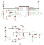
Yes, those components are snubbers. It's one of the last things to worry about and may not be necessary in the end, but I thought I'd draw them for completeness. When the diode is reverse biased it acts as a capacitor which resonates with the leakage inductance of the transformer, this isn't something unique to flyback converters or even SMPS, and you do have a choice of how to snub this, what's shown is just a common way. The snubber resistor is equal to the resonant impedance of the ringing parasitic L and C, the capacitance blocks DC across the snubber resistor and is generally 5-10x the ringing C so as to make its impedance negligible at the resonant frequency compared to the resistor. C10/11, R12/13 and D5/6 are a voltage clamp (essentially mini flyback converters with the resistor as the load) to stop the drain voltages flying back too high as to damage them, but really with such a low battery voltage, you'd likely be better off just buying some cheap voltage headroom on the transistors and forgetting the clamp.
 

KX36

New member
Small correction, the highest ripple current is at D=0.5, at which you need 278mH inductor.

Sorry about that, I'm used to forward converters, where Dmax=0.5, so didn't think about what happens as D increases further. That's what I get for writing that at 1AM after a 12 hour shift.

Also the key point you'll have to address is that push-pull converters are succeptable to flux walking and you will have to do something to avoid that, likely change topologies or change to current mode control. The schematic I gave is just an example of a more traditional UC3525A voltage mode setup and a more traditional push pull plant. It doesn't mean those 2 can just go together like that. You might, for example, change to current mode control with a UC3845 peak current mode controller followed by a UC3706 single ended to push-pull driver. Otherwise you might want to use a forward converter with a reset winding tailored for a Dmax of up to 0.7 or a half bridge converter which works well on voltage mode control, or as I say there's always boost and flyback converters but their non-linear conversion ratios make wide output ranges less feasable.

Anyway, always double check your work when possible, I use LTSPICE for that.
 
Last edited:

phaedrus

Member
I am unclear on some parts of your schematic:
1)Suppose R6(in your schematic) is turned to one end,so that it is a short to ground,wouldn't the output from the converter go to a maximum PWM and lose regulation ?
2) I assume D3 and D4 should be zener diodes(to clamp the Vgs) and mounted directly between gate and source ?

I did try using LTSPICE before ,but I seldom get meaningful results,maybe because my modelling of the transformer is not all that correct.I will have another try at it though.

Thanks again.
 

KX36

New member
Yes, as you rightly observed, you would want a fixed resistor in series with the variable resistor to limit how high the output voltage can go. I just drew it as it is as a simplified way of showing where the variable resistance should be. In the below circuit, you may have a 2k resistor in series with 20k pot, although these are rounded values.

D3 and D4 are schottky diodes to clamp the gate drive voltage positive. Because of the high switching speeds into the gate capacitance, there's a significant AC current into the gates and the energy stored in the gate capacitance when released can pull this node negative, damaging the IC. It's a standard IC protection diode and should be mounted as close as possible to the IC. You'll see them in many application notes and datasheets, often with another reverse biased schottky between pins 11 and 13 to clamp it to less than the positive rail. You may also see them on many CMOS ICs circuits as latchup protection.

I've designed a compensator for my example values as above. The L and C values are a little different as I added a few mA output for the resistive divider. All this high voltage low current work is bizarre. You shouldn't just use my values though, you should work it all out for yourself.


The key performance indicators are the crossover frequency (Fc) is 4.8kHz, phase margin at Fc is 68 degrees, gain margin is 24dB at 39kHz, gain at switching frequency is -44dB, gain at 1Hz is 75dB, the lowest the phase margin goes in the area of gain>1 is 60 degrees at 1.1kHz. This all says it should have good DC regulation and be completely stable. It's slightly underdamped and the zero and pole could be moved closer together for a better transient response, but I was only stabilising rather than optimising the loop and that's personal preference. There is a snubbing capacitor which will slow down the transient response significantly as it adds so much to the output capacitance. It just damps the LoCo resonance and so keeps the phase margin higher at this frequency. It's not strictly necessary and you could do all these calculations again without it, then you'd need to be confident Lo's series resistance and Co' ESR sufficiently damps this resonance to keep the phase above 0 degrees at this point.

When I was first learning all of this it took me a lot of time and maths to derive the transfer functions for the plant, compensator, modulator and full loop before I could start to make my own stable designs, and it all came down to the Vin/Vosc term in these equations. A simple thing but if it's not right, the gains are offset and it crosses over at the wrong place. One of the biggest weaknesses of voltage mode control is that the gain is proportional to Vin, so this must be rock steady. You will eventually need to simulate and test everything at both extremes of charge on your input battery. Oh, and the Vosc=2.3V (peak to peak voltage of the PWM sawtooth ramp) is something I've previously calculated for the UC2525A, that the sawtooth operates between 1.0V and 3.3V. I haven't confirmed this and I only calculated it previously in the conditions I was personally looking at in a different project; it's crucial that it's right so that's one of the many things you'll have to investigate.

In case you were wondering, I'm doing all of this out of my own curiosity. I got into SMPS on the back of valve amps, always intending to do a high voltage supply but never getting round to it.
 

KX36

New member
And here's the switching model once it's reached a steady state set at 250V out. Remember this is all idealised and it doesn't model the transformer or any parasitics which might need to be snubbed. It's a buck converter. This is because the push-pull converter is buck derived so there's no need to at the complexity of modelling the transformer at first, just transform Vin through the transformer turns ratio. I.e. Vin, as the transformer secondary voltage, is what would be Vin*Ns/Np.

Note there's no current limiting and in this simulation, the inrush current peaks at 500mA (20x load current!!) In a practical converter you'd limit this at the very least with a soft start duty cycle limit, but a soft start won't help when the output voltage level is adjusted if the converter is already on and the soft start cap is fully charged. Output ripple voltage is 25mV under the conditions in this simulation and inductor ripple current is 6.8mA.

 
Last edited:

KX36

New member
Here's the LTSPICE files for the above for you or anyone who wants to have a play around.

I have noticed a bit of a minor wobble at 20kHz which I haven't tracked down the source of yet. It's probably nothing to worry too much about as the amplitude of this wobble is much less than even the switching noise. That sort of thing is often to do with sampling frequencies since the DC to DC converter is essentially sampling as its switching frequency, however that doesn't appear to be the case this time as the max timestep is 50ns, so the simulation is sampling at a higher frequency than the converter. It's also not fixed by increasing the error amp's GBWP or open loop gain, which often cures these things so it doesn't seem to be factitious. It might be something to do with the high Vin/Vosc meaning unconventionally most of the gain comes from the plant and at the crossover frequency the error amp actually has gain of <0dB.
 

phaedrus

Member
1) Regarding the construction of the inductor,would it need any additional winding between the layers or is the enamel sufficient ? Since the voltage potential between the windings would be low,I am assuming no additional insulation would be needed.
2) Is it needed to draw 2.5mA in the feedback for regulation ?In my "naive" prototype,I had used a feedback current of about 1mA and it worked quite fine,beyond 100V.
 
Top