6kW+ design project

prof.hell

New member
All,

I have a need for a 6kW+ SMPS @ 12v, < 300mv ripple, fully regulated, single rail.

The general direction:

  1. Standard 90 - 260V AC input
  2. Full Bridge PWM-based design with voltage mode control
  3. PFC input at about 0.95
  4. 90%+ converter efficiency
  5. Considering parts from Linear Technologies, IFR and Microchip
  6. Explore the possibility of digital control (perhaps two versions of the design)

This is for a commercial requirement, but I'd like to work on this in collaboration with everybody and publish the results.

Anyone up for this?
 

donpetru

New member
How much money are you willing to spend on collaboration? Or how much money you want to pay for build the SMPS prototype?
And what is the business area in which you operate? how much is the turnover per year (USD)?

Best Regard,
donpetru
 

prof.hell

New member
I was thinking of making this a community effort so that the end result is open sourced to everyone - schematics, PCB design, BoM sourcing and, in the case of digital control, the necessary firmware in whatever language it's written. If that's the case, then I don't see where the investment aspect comes into it.

If we are talking about building a prototype, then the amount spent would be directly proportional to timelines associated with achieving a working prototype, bearing in mind that solutions from the likes of Pioneer Magnetics and TDK are very competitive all the way up to 15kW and beyond.

PM me directly if this is a service you want to discuss on a commercial basis. There is scope for this.

Let's iterate some more thoughts ..
 
Last edited:

donpetru

New member
I was thinking of making this a community effort so that the end result is open sourced to everyone - schematics, PCB design, BoM sourcing and, in the case of digital control, the necessary firmware in whatever language it's written. If that's the case, then I don't see where the investment aspect comes into it.
You want this forum community to help with various tips, including making a SMPS schematic, and PCB, and you afterwards to transform the result into a commercial product? I think you're joking. Who do you think is stupid to do that.

If we are talking about building a prototype, then the amount spent would be directly proportional to timelines associated with achieving a working prototype, bearing in mind that solutions from the likes of Pioneer Magnetics and TDK are very competitive all the way up to 15kW and beyond.
PM me directly if this is a service you want to discuss on a commercial basis. There is scope for this.
I have noticed that you have not answered my questions in the first post above. This makes me think that your intentions are totally different (ie, in other words, you want to build the SMPS, if possible, free of charge). You have to remember one thing: a forum is a hobby forum, if you want a commercial product can discuss other terms, including PM me directly, or, you can access: www.elance.com
There you find people willing to do it on little money (there are exceptions), but the results can be in this situation, one big bull****. You must be aware that with little money, you do nothing right.
You have any idea how much cost SMPS 6kW project (including: test reliability, design schematics, PCB...) ???????? I think not. By the way, from which country are you?
 

prof.hell

New member
You want this forum community to help with various tips, including making a SMPS schematic, and PCB, and you afterwards to transform the result into a commercial product? I think you're joking. Who do you think is stupid to do that.

So let's get this straight: maybe I didn't make myself clear in the original posting. When I said commercial, I didn't mean it to be a product to be soled, but rather commercial grade.

I have noticed that you have not answered my questions in the first post above. This makes me think that your intentions are totally different (ie, in other words, you want to build the SMPS, if possible, free of charge). You have to remember one thing: a forum is a hobby forum, if you want a commercial product can discuss other terms, including PM me directly, or, you can access: www.elance.com
There you find people willing to do it on little money (there are exceptions), but the results can be in this situation, one big bull****. You must be aware that with little money, you do nothing right.
You have any idea how much cost SMPS 6kW project (including: test reliability, design schematics, PCB...) ???????? I think not. By the way, from which country are you?

I don't necessarily like your attitude or language, and I don't really know who you think you are. You know nothing about my background, the industry I work in or my level or eduction. So I suggest you take a step back and reconsider.

For your information, a 6kW PSU from TDK is under a $1,000 the way and quantity we buy.

Honestly; there really is one in every pack, and here's the proof.
 

donpetru

New member
I apologize to the language above. I just wanted to know if you have even a vague idea about what mean SMPS design. And, you say:
For your information, a 6kW PSU from TDK is under a $1,000 the way and quantity we buy.
Considering your statement from the above quote, I think you do not know what it means SMPS design.
So, for your general knowledge, one thing means the sale price (you mentioned) and anything else means SMPS design (there are two completely different prices).

For example, 6kW PSU from TDK that sells for $1,000, the SMPS design consisted of more than 100 000 USD. You think they have made ​​so many pieces, maybe put a production of 1000 pcs. (or more, I don't know exactly), which means TDK earn 1 million dollars from sales, but product design cost over 100000 USD (or around). After that, the rest up to $ 1 million consisted of: value parts, assembly costs and then, of course, profit.

I hope you're not mad at me, but by the way you discussed the issue believe that you are a student (or a man at the beginning of his professional career).
 
Last edited:

prof.hell

New member
Initial staps

So .. ignoring the noise that is now present on this thread, here's the initial steps, as promised, and this is going to be fully open sourced to everyone as the project progresses:

Input AC voltage (V[SUB]DC[/SUB]): 380V
Output Voltage (V[SUB]o[/SUB]): 12V
Maximum output power (P[SUB]o, max[/SUB]): 6,250W
Switching frequency (f[SUB]s[/SUB]): 100kHz
Duty ratio phase shift (D[SUB]e[/SUB]): 0.5

This is going to be a full bridge DC-DC converter, with ZVS at a fixed switching frequency, a blocking capacitor at the primary side to increase efficiency and a series LC resonant circuit. The overall efficiency is increased due to the free-wheeling interval being reduced.

Block diagram as follows:

SMPS-block.jpg

For the purposes of mode analysis (to follow), the following assumptions will be made:

  • Leakage inductance of the transformer will be ignored since it is very small compared to the magnatising inductance. Thus, the turn ratio of the transformer (n) will be worked out as the direct ratio of the secondary to primary winding count.
  • Switching MOSFETs are ideal switches except for their output capacitor and internal diode
  • The output voltage (V[SUB]o[/SUB]) is constant

I will upload the mode analysis and associated curves over the course of the next few days, work schedule permitting.
 
Last edited:

donpetru

New member
All the theory you exposed above sounds like a hypothesis of a university graduation project.

I still stand to think how to get you 380 VDC ??? You ever measured, basically, what is the value of the output voltage of a bridge rectifier, which apply 230 VAC on input ??? I think not, because mention those 380 VDC. That would be the first mistake.

This is going to be a full bridge DC-DC converter, with ZVS at a fixed switching frequency, a blocking capacitor at the primary side to increase efficiency and a series LC resonant circuit.
You want to build 6kW SMPS, supplied to 230VAC and a SMPS topology with capacitor at the primary side (LC resonant circuit). I think joking !!! But to make sure of that, shows you a detailed schematic about it (only the control power transformer SMPS is enough).

The output voltage (Vo) is constant
Constant output voltage ???? You must be kidding. By the way, what the difference in voltage between no load and load operation you've thought to get?
 

MicrosiM

Administrator
Staff member
if you are using a PFC, you will get a regulated 380VDC from 90VAC to 264VAC

however, at that power level, I think your best choice is to use interleaved PFC circuit, to reduce the size of inductors + smaller size + lower noise.

This project cannot be done in one step, And I am sure that you know, or at least recognize the cost of making prototypes and making this SMPS.

Regards
 

prof.hell

New member
if you are using a PFC, you will get a regulated 380VDC from 90VAC to 264VAC

however, at that power level, I think your best choice is to use interleaved PFC circuit, to reduce the size of inductors + smaller size + lower noise.

Indeed; what's been posted is a first bash at requirements. Further iterations will consider different approaches to power factor corection.

This project cannot be done in one step, And I am sure that you know, or at least recognize the cost of making prototypes and making this SMPS.

Regards

Very true. The idea is to go through the motions of deriving, prototyping and designing a unit of this description, then go through validation ...etc. What started as a real need for satisfying a high-performance computing requirement has now already been fulfilled elsewhere; but the fun and usefulness of the project remains, methinks, and I'm still adament to go through with it and release it to the world.

By the way, I've read a few of your posts and liked what I read :)

Keep it up ..

All the best ..
 

MicrosiM

Administrator
Staff member
Indeed; what's been posted is a first bash at requirements. Further iterations will consider different approaches to power factor corection.


Very true. The idea is to go through the motions of deriving, prototyping and designing a unit of this description, then go through validation ...etc. What started as a real need for satisfying a high-performance computing requirement has now already been fulfilled elsewhere; but the fun and usefulness of the project remains, methinks, and I'm still adament to go through with it and release it to the world.

By the way, I've read a few of your posts and liked what I read :)

Keep it up ..

All the best ..


I really like to see you working around such project, if you look carefully for the correct circuits you need, your road to success will be short.

If you are still interested into this project, and still want it to become real, I can offer some help in the PFC stage, but I may not be able help in the regulated SMPS section, that's going to be somehow challenging task, but its not impossible.

I don't know if you have access to the parts needed, inductors, Mosfets, IGBTS, PFC controllers etc...

Again, I really like to see such project to become reality. And I will help you as much as I can.


Good luck
 

prof.hell

New member
I really like to see you working around such project, if you look carefully for the correct circuits you need, your road to success will be short.

If you are still interested into this project, and still want it to become real, I can offer some help in the PFC stage, but I may not be able help in the regulated SMPS section, that's going to be somehow challenging task, but its not impossible.

I don't know if you have access to the parts needed, inductors, Mosfets, IGBTS, PFC controllers etc...

Again, I really like to see such project to become reality. And I will help you as much as I can.


Good luck

Hi MicroSIM,

Much obliged for your response. Be great if you can take the PFC component in your strides, and I'll work on the rest. If anyone's interested in joining in, then of course the invitation is open.

Re: inductors and other components, my company has accounts with Arrow, Mouser and DigiKEY, so can source them relatively easily. If we hit an obstacle, I can always go direct to the manufacturers through existing contacts.

So .. here's the next instalment: theoretical waveforms and calculations.
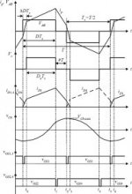
full-bridge-waveforms.jpg

For those up-tight folks, these graphs correspond to the assumptions list made earlier in the post; for completeness, the analysis will assume the following for the sake of simplifying the maths:


  • The transformer has the magnetising inductance Lm and a leakage inductance Lr that can be ignored, because it is very small compared with Lm. The turn ratio of the transformer is n
  • Switches are ideal components except for its output capacitor and internal diode
  • Output voltage Vo is constant


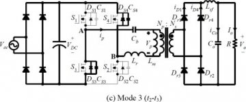
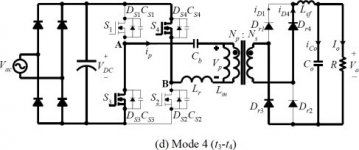
The modal derivation divides time interval T into four intervals: Powering (1), Freewheeling, Regeneration, Powering (2). We shall refer to these as Mode 1 - Mode 4.

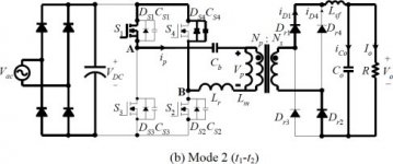
The equivalent circuits for these modes, which maps to the above waveforms, are as follows:
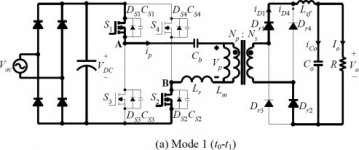
mode-1.jpg

mode-2.jpg

mode-3.jpg

mode-4.jpg

The mathematical derivation for each is as follows:


  • Mode 1 (t0 - t1): This is the first powering interval, which starts at time t=t0. Power is transferred from the primary to the secondary windings through switches S1 and S2, which are are turned on at ZVS. At this point, secondary bridge rectifier diodes Dr1 and Dr2 are turned on, while diodes Dr3 and Dr4 are turned off. Output voltage Vois is reflected to the primary and the primary, hence current ip charges the blocking capacitor Cb. Thus, the blocking capacitor voltage vCb increases nonlinearly. The average voltage of vCbis negative during this mode. As a result, bridge voltage VAB is increases. The primary current ip and the blocking capacitor voltage vCb are expressed as follows:

    (got to go to work .. rest to come :))
 

prof.hell

New member
OK .. so picking up where I left off earlier ..

  • Mode 1 (t[SUB]0[/SUB] - t[SUB]1[/SUB]): This is the first powering interval, which starts at time t=t0. Power is transferred from the primary to the secondary windings through switches S1 and S2, which are are turned on at ZVS. At this point, secondary bridge rectifier diodes Dr1 and Dr2 are turned on, while diodes Dr3 and Dr4 are turned off. Output voltage Vois is reflected to the primary and the primary, hence current ip charges the blocking capacitor Cb. Thus, the blocking capacitor voltage vCb increases nonlinearly. The average voltage of vCbis negative during this mode. As a result, bridge voltage VAB is increases. The primary current ip and the blocking capacitor voltage vCb are expressed as follows (sorry for pasting the equation as an image; not worked out of BB Code has support for math functions yet):

    mode_1_eqn.gif
    mode_1_eqn_2.gif

    This mode ends with S[SUB]2[/SUB] being turned off at t=t[SUB]1[/SUB]
 

prof.hell

New member
(IMPORTANT: I missed a term of the Mode 1 equations in the Math BB code, so redoing it for completeness. Apologies).

  • Mode 1 (t[SUB]0[/SUB] - t[SUB]1[/SUB]): This is the first powering interval, which starts at time t=t0. Power is transferred from the primary to the secondary windings through switches S1 and S2, which are are turned on at ZVS. At this point, secondary bridge rectifier diodes Dr1 and Dr2 are turned on, while diodes Dr3 and Dr4 are turned off. Output voltage Vois is reflected to the primary and the primary, hence current ip charges the blocking capacitor Cb. Thus, the blocking capacitor voltage vCb increases nonlinearly. The average voltage of vCbis negative during this mode. As a result, bridge voltage VAB is increases. The primary current ip and the blocking capacitor voltage vCb are expressed as follows (sorry for pasting the equation as an image; not worked out of BB Code has support for math functions yet):

    mode_1_eqn_1.gif
    mode_1_eqn_2.gif
  • Mode 2 (t[SUB]1[/SUB]-t[SUB]2[/SUB]): This is the freewheeling interval, which starts at t = t1. At this point in time, switch S[SUB]2[/SUB] turns off, parasitic diode D[SUB]S4[/SUB] of switch S[SUB]4[/SUB] turns on. The power transferred from the primary to the secondary flows through the secondary diode D[SUB]r1[/SUB] and D[SUB]r2[/SUB], and then the parasitic capacitor C[SUB]S2[/SUB] of switch S[SUB]2[/SUB] is charged. The energy of blocking capacitor C[SUB]b[/SUB] and resonant inductance L[SUB]r[/SUB] both discharge parasitic diode C[SUB]S4[/SUB] of the switch S[SUB]4[/SUB]. Subsequently, switch S[SUB]4[/SUB] turns on with ZVS. In this mode, the slope of the primary current i[SUB]p[/SUB] decreases more quickly than a comparable conventional converter without the blocking capacitor C[SUB]b[/SUB], since then the energy circulated by the freewheeling current also decreases quickly. The primary current i[SUB]p[/SUB] is given as follows:

    mode_2_eqn_1.gif

    This mode ends when switch S[SUB]1[/SUB] turns off at time t = t[SUB]2[/SUB].
 

prof.hell

New member
Hi Mario,

Nice work.

Care to join in and work on this project? I'm currently doing the derivation and converter parts, while MicrosiM has offered to work on the PFC section.

See what takes your fancy ...

Ahmed.
 

MicrosiM

Administrator
Staff member
Hi Mario,

Nice work.

Care to join in and work on this project? I'm currently doing the derivation and converter parts, while MicrosiM has offered to work on the PFC section.

See what takes your fancy ...

Ahmed.

I said I will provide help, I cannot work directly over this project, as it will consume my time, money, Also requires lot of effort.

I only can give some advices, hints etc...

Sorry for that.
 
Top