SG3525 Driver Circuit

twenglish1

New member
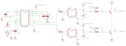
I came up with the gate drive circuit for experimenting, and i will probably need to make some changes to it before i actually try and build it, i am still a little iffy understanding how the SG3525 feedback works, i based the SG3525 portion of the circuit off of schematics found online and the data sheet, i understand how the error amp works but i am not entirely sure how to build a feedback circuit to vary the duty cycle based on say a variable resistor, that is what i would like to do, maybe someone can help me? also are there any obvious problems with the circuit i made?
 

KX36

New member
I think those gate drivers need a power supply across pins 5 and 8 and the gate output is pin 6-7. In the case of the high side driver for Q1 you'd need that supply to be floating and referenced to q1's emitter on the Vee pin, rather than ground referenced.
 

twenglish1

New member
I'm not sure what happened from when I drew it to exporting the image, but the igbt bases were meant to be on pins 6 and 7 of the drivers, and thanks for pointing out about my mistake with the high side driver. So it is ok for the "gate supply 2" to power both the low side driver and the sg3525?
 

KX36

New member
Yes, that should be OK assuming the rail voltage is suitable for both, just make sure there's enough decoupling capacitance around each IC. The high side gate supply can probably be a diode capacitor bootstrap circuit as IR2110/IR2113 would have used.
 

twenglish1

New member
So you're saying instead of the two separate supplies I can use one and just design a bootstrap circuit for the high side and it will work with the hcpl3120? And what does the rail voltage need to be suitable for? The hcpl3120s?
 
Top