You are using an out of date browser. It may not display this or other websites correctly.
You should upgrade or use an alternative browser.
You should upgrade or use an alternative browser.
0~500V SMPS based on SG3525
- Thread starter phaedrus
- Start date
I don't think you'd need extra insulation in the inductor between layers of turns if the rest of the inductor design's OK. We're talking about 10x the voltage and many more turns than I'm used to so take this with a pinch of salt, but I don't think you should need to take any extra precautions compared to winding a mains transformer's primary.
Regarding the current through R1, I didn't optimise it as my design is for illustrative purposes only. Resistors can only be so high resistance to be practical. Normally the error amp will have some gain, so R2 will be higher resistance than R1. You also can't make resistors so big as to introduce an error due to the opamp's input bias current.
While we're talking about load currents, here's an important point: power supplies need a minimum load. I didn't really make it obvious, but we've been designing for continuous inductor current (CCM). The loop transfer function changes if it drops into DCM which at best changes the transient response of the power supply and at worst can cause instability. If the load is too low it will drop into DCM or, taken to the extreme with too little load at all to discharge the capacitor, the capacitor voltage can rise but cannot fall so you can imagine what happens to the output voltage over time. We designed a ripple current of 20% max DC current, so to keep it in CCM, we need a minimum DC load of half this peak to peak current, which is 10% max DC current (works out as 3.5mA min load at Vout=278V, D=0.5 in my design as I added some wiggle room to your specified output current). Your output current is so low that if you had a fixed output voltage, you could save yourself some components and make this minimum load current pass through R1.
Unfortunately you'd have to design this for worst case conditions of ripple current and output voltage, which means that if you just used a resistive load under different conditions it will be drawing significantly more than the desired minimum load, so you may have to put in a simple constant current sink.
Some trials
Hi Gentlemen,
I built up a circuit, and did some trials.
At lower voltage the performance is extremely poor and improves as the output voltage is increased.I have attached the ckt diagram , and some sketches of the waveforms as seen on the scope.
As the output voltage is increased,the performance improves substantially. At a set value of 400V,the voltage (under 10k load)drops by 20V,but there is absolutely no ripple (with load and w/o load).
At 270V there is no ripple without load,but under load (10k) there is a ripple of 50V.
At 50V ,it is absolutely horrible with waveform attached.
Let me know if any further details are needed for analysis.
Hope to have your comments and suggestions.
Cheers.

Importance of proper compensation n/w
Hi ,
Now I am getting proper results after changing the compensation network to the one as mentioned in Matt Helyar's simulation.Previously I had used the components as mentioned in a website.
I had to use slightly different values,due to availability of components,but I am getting much better results.
There is no ripple throughout the range from 50V~400V with and without load.I tested 50V @ 60mA. 400V was tested @ 40mA,it dropped to 380 on load,which is acceptable.
Thanks Matt !!
glad things are working better! with the ripple voltage you described I wouldn't be surprised if that was actually oscillation rather than just ripple, so it looks like by improving the compensation you've improved stability.
IIRC, the IC has totem pole drivers on the outputs, so should be able to drive the transistors without a separate driver IC. you may also be able to reduce the drive requirements by using different transistors, but the difference probably wouldn't be massive and they're probably fine as they are. have you tried without the driver IC? transistor gates and drains are useful places to probe with the scope to see what's going on.
Matt
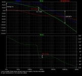
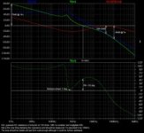
I put your compensator circuits into the earlier SPICE simulation and here are the resulting Bode plots annotated with what we discussed in PM. I've made a guess at the DC resistance of your inductor based on a different inductor's datasheet, this resistance is the only thing really damping the LC resonance, so you should check it. You can always add the RC snubber in my earlier post to damp this resonance if you find it necessary.


The first picture should be your unstable first attempt, the second is your stable second attempt. Hopefully you should see why you can't just google for a "one size fits all" compensation network for the error amplifier, you have to design the compensation to match the plant gain to your desired loop gain criteria.
P.S. IMHO, I don't really like these overly split up schematics. It's OK to a point if your design is complex and modular, but it's a simple schematic and could probably be clearler if it was drawn in 1 piece. e.g. you have your compensator split between 3 sections in one schematic and R12 is duplicated. That's just me splitting hairs though.
After what I said about the choice of transistors, the ones you have look quite well suited to the task. The relatively low drain voltages should reduce the miller capacitance and so make them even easier to drive. Also, what's the tranzorb/schottky pair thing on the inverting input doing? Overvoltage protection? I would try to avoid adding any protection circuitry that may introduce parasitics which affect the loop when reverse biased or which may open the feedback loop and cause havoc when forward biased. Or have I misunderstood. There are better ways of implementing overvoltage/overcurrent protection.
Matt
Attachments
-
 High voltage low current VMC type III linear - phaedrus.jpg18.9 KB · Views: 33
 -
 High voltage low current VMC type III linear - phaedrus2.jpg18.9 KB · Views: 18
Thanks much for your continued interest.
1) I will try without the driver IC and let you know shortly.
2) The inductor DC resistance is actually ~ 9 (nine) ohms. I had wound it using a RM7 core,about 300 turns of SWG36.What would be the manifestation of the resonance which you mention ?
3) The transzorb/schottky pair is "supposed" to provide some clamping protection in case the lower arm of the resistive divider opens out or to avoid an initial pulse,due to the parasitic capacitance of the HV 200k resistor.
After a some reading I am bit more clear on the relevance of phase margin and gain margin to stabilizing the control loop.
You mention DC gain at 1Hz is sub optimal,what is optimal and what would be effect of this ?Also what is the relevance of the gain at the switching frequency ?
Usually no one sees my schematics other than I,hence the drafting sometimes gets a bit shabby") .
.
1) I will try without the driver IC and let you know shortly.
2) The inductor DC resistance is actually ~ 9 (nine) ohms. I had wound it using a RM7 core,about 300 turns of SWG36.What would be the manifestation of the resonance which you mention ?
3) The transzorb/schottky pair is "supposed" to provide some clamping protection in case the lower arm of the resistive divider opens out or to avoid an initial pulse,due to the parasitic capacitance of the HV 200k resistor.
After a some reading I am bit more clear on the relevance of phase margin and gain margin to stabilizing the control loop.
You mention DC gain at 1Hz is sub optimal,what is optimal and what would be effect of this ?Also what is the relevance of the gain at the switching frequency ?
Usually no one sees my schematics other than I,hence the drafting sometimes gets a bit shabby
.With too little damping on the LC filter, the gain peak will be higher and the phase will drop below zero near this frequency. It's not as bad as having no phase margin at crossover, but it is possible to get oscillation under some circumstances as there is significant gain at this frequency.
I'd probably just use a diode to clamp pin 1 to pin 15 if I was worried about overvoltage on that pin, but I see no reason why R12 would come open, even as a variable resistor if it's wired correctly with the resistive element wired like a fixed resistor and the wiper tied to one end. I suppose if you turned the output voltage down too quickly while it was running, the voltage at the pin might rise before the output capacitor discharges.
Gain at 1 Hz is not really significant in itself, its just the lowest frequency I plotted to give an indication of DC gain. The higher the DC loop gain, the better the DC regulation. 55dB gain here is adequate, but that all comes from your unusually high input voltage giving your plant high DC gain, only 7.5dB comes from the error amp. in a different circuit, this might result in low loop DC gain and unnecessarily poor regulation. With a capacitor blocking DC from the error amp's local feedback path, the DC gain of the error amp tends towards its open loop gain. It's irrelevant if the loop is unstable though.
I think the compensation you originally had came from a current mode controlled (CMC) power supply. The plant gain in CMC is very different as it by design approximates a current source into the output capacitor, so that gives high DC gain reducing the need for extra DC gain from the error amp. Of course, you can still include this extra capacitor in CMC loops for extra DC gain and type II compensation is common in CMC loops. In the ubiquitous TL431/optoisolator (which is a surrogate voltage error amp) in most power supplies you might see a capacitor between reference and cathode pins and that's what it's doing.
This is my understanding, and it's probably an oversimplification, but... The loop gain is a measure of the loops ability to perform its duty of regulation. DC gain is high, so you get good DC regulation; gain around 50-120 Hz is high, so noise from rectified mains is regulated away by negative feedback etc. However the PWM is essentially sampling the voltage at the switching frequency, so you don't want it trying to compensate for the switching noise as it's not sampling it fast enough for the PWM to deal with it. See Nyquist Frequency. As well as this, frequencies which have negative phase margin and a gain of not far below 0dB might ring on stimulation even though they wont oscillate and the switching noise in a practical circuit can be quite a stimulus. For these reasons, you want it to ignore frequencies above half the switching frequency and crossover is normally set between 5-20% of switching frequency, often with the compensator's pole around half switching frequency.