Hi, I'm new here and just found this forum about 2 weeks ago with lot of great threads about how to build custom SMPS. I'm currently developing an ON-LINE UPS for server rack and the goal is to make it in the most simplest way which I think is with a micro controller. The Inverter which would run from the power supply 24/7 is capable of outputting 3.5kW and requires DC24V for the operation. The problem is that on full load this means more than 150AMPs from the DC line which is in parallel with two 200Ah SLA battery which at the same time needs to be charged while the AC line is present. I have some components that could be useful to build the power supply and I used these to make the schematic that I posted in the attachments.
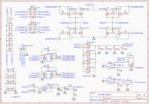
The idea is that there is an auxiliary power supply (I used the TOPSwitch277 and it's basic schema to make it) which provides DC12V which powers the system while the main power supply is not in use but the system also uses the main supply as secondary so the MCU is powered from the "redundant low power line". I used my basic knowledge of SMPS to design this thing so excuse my for my mistakes So the system looks like this, AC goes through the filtering stage then rectified by a full bridge rectifier, then fed to a capacitor bank and then into the IGBTs in Full Bridge configuration which are driven by two IR2106s and there would be a custom high frequency transformer to step down this high voltage dc. Then there are four schottky diodes to rectify this voltage at the output. To tell the MCU about the output current I used an ACS758 current sensor module and the output voltage would also be measured by the MCU on the DC line. The MCU provides the four PWM signals for the mosfet drivers.
What frequency and duty cycle would be ideal to use with this configuration and what should the MCU do when current rises or falls down to keep the ouput dc voltage from dropping?
What are the parameters of the transformer which is capable of delivering this much current constantly?
How can I eliminate the noise from the power supply both dc and ac line?
Also would this even work?
Excuse my for my English and my mistakes with this thing.
All helps are welcome and I'm open to any suggestion which helps me to improve this design.
EDIT
I'm really new here, somehow the attachment is resized and could not be seen correctly so I uploaded it onto Mega.nz
The idea is that there is an auxiliary power supply (I used the TOPSwitch277 and it's basic schema to make it) which provides DC12V which powers the system while the main power supply is not in use but the system also uses the main supply as secondary so the MCU is powered from the "redundant low power line". I used my basic knowledge of SMPS to design this thing so excuse my for my mistakes
So the system looks like this, AC goes through the filtering stage then rectified by a full bridge rectifier, then fed to a capacitor bank and then into the IGBTs in Full Bridge configuration which are driven by two IR2106s and there would be a custom high frequency transformer to step down this high voltage dc. Then there are four schottky diodes to rectify this voltage at the output. To tell the MCU about the output current I used an ACS758 current sensor module and the output voltage would also be measured by the MCU on the DC line. The MCU provides the four PWM signals for the mosfet drivers.What frequency and duty cycle would be ideal to use with this configuration and what should the MCU do when current rises or falls down to keep the ouput dc voltage from dropping?
What are the parameters of the transformer which is capable of delivering this much current constantly?
How can I eliminate the noise from the power supply both dc and ac line?
Also would this even work?
Excuse my for my English and my mistakes with this thing.
All helps are welcome and I'm open to any suggestion which helps me to improve this design.
EDIT
I'm really new here, somehow the attachment is resized and could not be seen correctly so I uploaded it onto Mega.nz
Attachments
-
 Capture.jpg19.8 KB · Views: 63
Last edited:
