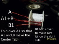
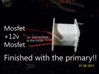
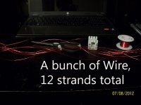
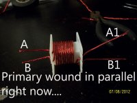
I've been crazy busy lately and haven't been able to work on this as much as I would like, but I am gonna try and take another stab at the transformer today and see what I can get. Norazmi has given me some great advice with how to wind this thing properly so I'll be trying it later. More updates soon!!
You are using an out of date browser. It may not display this or other websites correctly.
You should upgrade or use an alternative browser.
You should upgrade or use an alternative browser.
12v 250w Car SMPS based off SG3525
- Thread starter codex653
- Start date

I'll be sure to test that on the mosfets. What is the reason behind the voltage between gate and gnd needing to be between 3-4.xx volts?? I know in BJT transistors a bias is needed on the base for correct operation (in some applications). Is it kind of the same sort of thing here even though mosfets work differently?
I'll try and remember to post waveforms as well
I'll try and remember to post waveforms as well
aha, there u have problem... , look at datasheet, mosfet only can hold 5v max between gate to drain, some can hold 2-4vdc. If voltage more than that, mosfet will go crazy and overheat, thats why u have problem with overheat situation. check your component value.. traces... and others.
look at datasheet, mosfet only can hold 5v max between gate to drain, some can hold 2-4vdc. If voltage more than that, mosfet will go crazy and overheat, thats why u have problem with overheat situation. check your component value.. traces... and others.
are you sure??? I checked the datasheet for the IRF540N and the max voltage between gate and drain is 100v..the gate to source max voltage is +/- 20v...the only thing I see that is 2-4v is the threshold level, which all that means is the voltage level where the mosfet switches from off to on and vice versa correct?
DCPreamp
New member
Hi codex653,
I'm not sure what norazmi is talking about. The whole idea of PWM is to run a square wave from the current-boost transistors to the Gate of the FETs, through a current-limiting resistor, which swings from 0 to Vcc (12-14VDC). Driving a FET's Gate with 2-4VDC will only partially turn it on (active region) and it will blow or get super hot. I've built lots of SMPSs and that's always the case using FETs as switches; 0VGS = open and 12VGS = saturated.
Maybe he means using a DMM on AC setting and getting a reading of 2-4V, but only because it's a ratio of off-to-on time giving a lower average voltage.
Anyway, you're right about the +/- 20VGS to drive the FET and the 100VDS breakdown voltage. I'm sure norazmi will explain further or he will provide additional info.
As far as the Gate resistors you were talking about, I always use 10ohm resistors. They've always worked fine, limited inrush current into the Gates of the FETs, and switched them plenty fast enough for efficient operation. I once used some 100ohm resistors for Gate drive, but once the SMPS got really hot, the FETs blew. It seems the hot FETs Gate capacitance went way up causing severe slewing and blown FETs. You can play around with the Gate resistor values for optimal performance, but I wouldn't go too high. Just my two-cents.
Are you using Sprint Layout 5 for your PCB design? If so, can you post the .Lay for the board design? I'd love to check it out! If not, then don't worry about it. Nice SMPS by the way! Thank you for making all your work public for our learning. It's much appreciated! I'm new here, so I'm still poking around learning the in-and-outs of the forum. But I have a lot of experience and hope I can help! I also have a few SMPS's I've designed and built and can post the project details for everyone's review.
Thanks for the reply! Yah I was kind of wondering where norazmi was going with that as well.
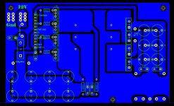
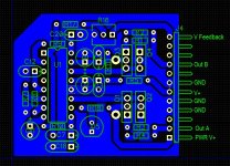
Sprint Layout 5? I'm guessing that is some sort of pcb layout/manufacturing program? I've been using DipTrace as I like the simplicity and look/feel of the program. I've posted my design for the pcb before, but that was several pages back and I don't feel like making you go and search for them so I'll just post em' again. I have two boards I designed. The first you see is the driver board which is mounted vertically on the main board.
I'm thinking that the problem may lie in pcb design...I've never had a class or anything on doing proper layouts for high frequency high current designs so I'm willing to bet there are areas I need to improve on my design. Do you have suggestions? You seem to be well versed in the area of SMPS's
Sprint Layout 5? I'm guessing that is some sort of pcb layout/manufacturing program? I've been using DipTrace as I like the simplicity and look/feel of the program. I've posted my design for the pcb before, but that was several pages back and I don't feel like making you go and search for them so I'll just post em' again.
I have two boards I designed. The first you see is the driver board which is mounted vertically on the main board. I'm thinking that the problem may lie in pcb design...I've never had a class or anything on doing proper layouts for high frequency high current designs so I'm willing to bet there are areas I need to improve on my design. Do you have suggestions? You seem to be well versed in the area of SMPS's
Attachments
-
 Final SMPS Board.JPG102.5 KB · Views: 102
 -
 Final SMPS Driver Board.JPG145.4 KB · Views: 104
DCPreamp
New member
DIP Trace is cool - I've used it before too. Sprint Layout 5 is a full-featured PCB CAD program for less than $50 and it outputs all the necessary Gerber files necessary for professional PCB manufacturing. It can print nice layouts too for home etching - like you do. It will also output a file format for milling PCBs with CNC machines - something I hope to do some day. Anyways, it's cheap and works great. (I'm just endorsing it because I like it - I'm not with the company in any way FYI).
You have some sort of weird problem. Previously, you said the frequency dropped from 50K to 11K (approx.). Because yours is a driven supply, the frequency should never change! So something's affecting your driver IC - maybe your bench supply is going into current limiting momentarily causing glitches. Since you have a scope, look at the Vcc of the supply chip, look at the outputs of the driver IC, and at the outputs of the current-boost transistors. Make sure you have clean Vcc at around 12VDC. Also make sure the outputs from the IC are nice, clean square waves swinging from 0V to 12V and are the correct frequency. Same with the driver transistors - same clean signal and accurate frequency. Also look at your feedback signal and see if it could be causing your IC to reduce the PWM when it should not.
With everything you described, if the switching frequency dropped like you said, it will certainly run hot and draw lots of current because the core probably will not have proper inductance at low frequencies. Regarding the Gate drive resistors, values from 4.7 to 33ohms should not make that much difference. If it does, you may have some or all bad FETs. Without the FETs in the PCB, you could place some 4.7nF caps in the Gate-Source locations to simulate the Gate capacitance of the FETs without risking blowing anything up. Once you're satisfied with everything and it's all working perfectly, you could then add the FETs and proceed.
Let us know what you find. I'm very interested to know what's going on! I'll post another reply with some comments about your PCBs. Excellent work so far, though!
I'm typing this on my phone so this will probably be short and sweet since I have no keyboard. If I remember correctly, I said that the frequency dropped at the drain of the mosfets...or at least I hope I clarified that point. The gate signal was a steady 50Khz clean square wave. It was the drain that had the funky looking wave forms and had the frequency drop which made me be suspicious about the driver circuit not being able to drive the mosfets properly. At that moment I did not have any resistor/cap to clamp down on the inductive spikes from the switching. I have yet to try the latest transformer I wound thanks to being so darn busy with work. Maybe I will find time to try tomorrow.
DCPreamp
New member
Okay, that clears things up a bit. Sorry I missed the details about the frequency being on the transformer side. Still, if you have a good, clean, 50KHz, 0 - 12V square-wave at the Gate resistors or on the Gates of the FETs, then I suspect you have a transformer or MOSFET (shorted D-S or leaky) problem.
You definitely need R-C filters on the Drains of the FETs to limit switching noise and spikes. Depending on their value, they will raise your idle current a bit, but it's worth the clean switching.
Does this sound reasonable? Does anybody else have suggestions for troubleshooting codex's design?
You definitely need R-C filters on the Drains of the FETs to limit switching noise and spikes. Depending on their value, they will raise your idle current a bit, but it's worth the clean switching.
Does this sound reasonable? Does anybody else have suggestions for troubleshooting codex's design?