ok yup I'm gonna try it later tonight if at all possible. Just off the top of your head, do you know the math to get the correct R-C filter values for the 50Khz? I believe i've read somewhere that the performance of the filter changes with the frequency so I want to optimize it as best I can. I'll also do a search on google.
You are using an out of date browser. It may not display this or other websites correctly.
You should upgrade or use an alternative browser.
You should upgrade or use an alternative browser.
12v 250w Car SMPS based off SG3525
- Thread starter codex653
- Start date
SUCCESS!!!!!  I put in the R/C filter and tested out my new "norazmi style" transformer and it worked flawlessly!! Atleast, that's under no load ofcourse ((@ but the point is, the mosfet's drain waveform was a good squarewave with no overshoots, ringing, etc. Although I may not be able to see that if it's there cause I don't exactly have a "normal" scope per say. It's a mini digital oscilloscope, but it does it's job well enough for me.
Ahhhh I'm so glad this worked! The R/C filter values were 10 ohm 1W for the resistors and 47nF 100v for the caps. Now its time to go and resize some things on my pcb...stuff just isn't fitting quite as nicely as I want them to on this prototype board.
I put in the R/C filter and tested out my new "norazmi style" transformer and it worked flawlessly!! Atleast, that's under no load ofcourse ((@ but the point is, the mosfet's drain waveform was a good squarewave with no overshoots, ringing, etc. Although I may not be able to see that if it's there cause I don't exactly have a "normal" scope per say. It's a mini digital oscilloscope, but it does it's job well enough for me. Ahhhh I'm so glad this worked! The R/C filter values were 10 ohm 1W for the resistors and 47nF 100v for the caps. Now its time to go and resize some things on my pcb...stuff just isn't fitting quite as nicely as I want them to on this prototype board.
DCPreamp
New member
Wow, fantastic job! You're nailing it down very well. As far as R-C filters for the Drains go, I do not know of an exact formula, besides a basic -3dB filter at 50KHz. But if you look at a number of schematics, you'll start to see a pattern of values very similar to the ones you used. You hit it exactly right! Of course, you can also play with those values to vary the switching performance. For example, you could lower the resistor to 4.7ohms or could increase the capacitor value to 680nF - either of those steps will increase idle current and will round-off leading-edge of the Drain switching waveform. Or, you can go the other direction, raise the values and lower the idle current and maybe end up with spikes on the Drain waveforms. So, it comes down to what the SMPS designer wants to do as the best trade-off of values to performance.
I agree with the transformer design. It looks fantastic and should perform extremely well. Ideal transformers have very tight, symmetrical windings, everything taped and/or epoxied down, copper shielding added around the periphery of the windings, and everything mechanically secured together.
As long as your scope has the resolution to show spikes, slewing, noise, and basic waveforms up to a few MHz, then it's more than enough for SMPS design!
What's your next step? Finish your board design? Maybe build a more complete prototype for some power testing?
Keep us informed as you progress. Again, excellent work!
Codex, sory i was busy lately with my younger sister wedding, ahh i`m very tired
Ah no worries
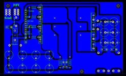
congrats on your sister's wedding! Here's a new revision of the pcb! Mostly what I wanted to change was the arrangement of the power semiconductors so that the screws were accessible from the outside as much as possible. Also I believe I lengthened the traces a little bit between the mosfets and transformer, but hopefully that wont prove to be adverse. I believe this new arrangement will work better? what do you all think? Old design first picture
Attachments
-
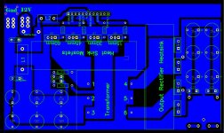 Final SMPS Board Rev 6.JPG132.3 KB · Views: 114
 -
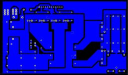 Final SMPS Board Rev 6 without silkscreen.JPG82.6 KB · Views: 102
 -
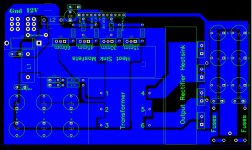
 Final SMPS Board.JPG102.5 KB · Views: 111
DCPreamp
New member
Here are some observations about your PCB design:
1) The ground plane around the Source leads seems thin. You can possibly connect it under L2 and again to the left of the rectifier heatsink. You may be keeping it separate on purpose for noise, but I think current capability is important. The ground is also thin under C26, C27, and C29 - you can probably shift the caps up towards C8, C25, and C28 and thicken the trace.
2) The R-C filters off the Drain leads are connected to V+, but should be connected to ground. It will work, but is not typically connected this way.
3) The ground plane between the V+/- secondary caps looks thin too. Seems it should not have that narrow channel between and below C31 and C21.
4) The grounds between the primary side and secondary of the entire supply should be split. It's typical to have the grounds separated for noise reasons and so that they will be connected by wiring in the completed and installed system.
5) The driver board's V+ and the PWRV+, passing through L2, should have an additional capacitor forming an L-C filter. The cap should be fairly large - ballpark like 220uF - and should even include a 100nF film cap in parallel to even further reduce noise on the V+ lines. I know you have some small caps on the driver PCB, but I would filter the V+ first on the main PCB.
6) You may want to add a set of pull-down resistors for the gates of each bank of FETs. That way the Gates are a) protected from ESD if the driver board is removed and b) it ensures the Gates are guaranteed low at all times. Just something like a 10K from Out A and Out B to ground. I always design circuits to be stable under many circumstances and two 1/4W resistors are cheap compared to four FETs or even a fuse.
7) You should really consider a large power diode across Vin to protect against reverse voltage being applied. It only needs to be large enough to handle the peak current (not continuous) to blow the fuse and would be connected with the cathode towards V+ and Anode towards Ground. Something like a 6A, 50V barrel diode will still momentarily pass 30 - 50A to blow the fuse protecting all your precious semiconductors!
Lastly, are you going to use the feedback input on the driver PCB for anything? If it is going to just be left floating there, just make sure it won't interfere with the circuit in any way and is quite immune to noise. You may want to add a jumper or something to have the option of shorting the pin to ground or something just so you can be sure everything is stable under all conditions.
I hope this is not too much to list. But look through my list and if you've already addresses things, then just disregard my suggestions. But for a dependable, robust supply, most of what I listed are pretty good routine items to add to any SMPS. Fantastic job, by the way!
DCPreamp
New member
It's my pleasure to be able to help! But, don't worry, when I do my next project (currently scheming with my evil brain...), there'll be plenty of opportunity to help back!
So did my suggestions make sense? If you have any questions about anything, let me know and I can go into more detail as needed.
Regards,
So did my suggestions make sense? If you have any questions about anything, let me know and I can go into more detail as needed.
Regards,
DCPreamp
New member
Fantastic design changes! Considering your work situation, you're making great progress on your SMPS!
Here's a couple new observations:
1) The ground connection at the - (negative) junction of C1 & C2 is not connected. It just needs a trace from the - junction to the large ground-plane just to its left.
2) The secondary's center-tap ground, pin 5, is still connected to the primary-side ground and not to the secondary's, capacitor ground (it's just floating now). It just needs to be routed and connected to Pin 5.
Otherwise, it looks great! I think you're there and ready to take the next step and wrap this baby up and put it into service! That's the real excitement of building a DIY project - when you put it to work and it does everything exactly as you designed it to do. It's the moment of truth, but sadly, can also be the moment when your project you've worked so hard to build, can go up in flames or just die quietly with just a tiny whiff-of-smoke. I've had both occur, but luckily as my skills have advanced, the ratio of success-to-failures has increased dramatically. Yea!
Let us know when you finish the next round of mods. Outstanding work!
. Yup I was gonna use those standard "T" shaped heat sinks you always find in smps's but I found them to be much too flimsy and would start to bend ally mosfets leads. So I opted for ones with a wider base for support.codex, output rectifier heatsink size can be reduce to save some space
Dcpreamp- gosh dangit how can I keep on seeming to neglect those darn grounds!
I'll make that fix and get to building it today!! Pictures to come of the build later! BAM! it works!! Put everything on there (which fits very nice and snug i might add), and tested it out! Got a nice clean waveform on the primary side, didn't really bother checking the secondary waveform cause I know what it's gonna look like, and I have a symmetrical +/- 36.7vdc on the output!! I have yet to test the power capabilities of it yet as well as testing out the regulation controls, but I'll get to that tomorrow. I have to go work now ::SD
Hopefully I'll get some pics up later tonight?? Not sure...
I have yet to test the power capabilities of it yet as well as testing out the regulation controls, but I'll get to that tomorrow. I have to go work now ::SDHopefully I'll get some pics up later tonight?? Not sure...
DCPreamp
New member
BAM! it works!! Put everything on there (which fits very nice and snug i might add), and tested it out! Got a nice clean waveform on the primary side, didn't really bother checking the secondary waveform cause I know what it's gonna look like, and I have a symmetrical +/- 36.7vdc on the output!!
Hopefully I'll get some pics up later tonight?? Not sure...
Fantastic news! The thrill of designing, prototyping, building, and testing a DIY project! It's a thrill most non-DIY'ers will ever know. I've been fortunate enough to have experienced that a few times and I still love and strive for it!
Looking forward to seeing the completed supply and reading its performance numbers. Thanks again for including us in your design. Thank you also for being open to input and feedback! Will you be posting a schematic of the final circuit?
yah I don't know when I'm gonna get around to that final circuit schematic Tested it out today and found out it works decently well up to about 60w and then things really start to freak out. The power supply is at 14v and when drawing 4A on the primary side, everything seems to be ok. Waveforms are good, mosfet's heatsink is getting a bit warm, but nothing concerning. Then I hit around 7A and my mosfets started REALLY heating up and my scope was showing some major spiking on the primary waveform. The snubber network resistors are getting VERY hot and i'm pretty sure that isn't supposed to be happening. I know they dissipate a little bit of power, but they are 1 watt resistors and are heating up as if they are eating 2 or 3 watts!
On the plus side of things, my output rectifier and capacitors don't heat up...gotta look for at least one small victory hah Could it be that my gate resistors are too small? I reverted back to 10 ohms on this build. I believe i heard it said somewhere that if the gate resistors are too low then when you get into a higher current range the mosfets will start to misbehave? Can't quite be sure if i'm recalling that right...
Tested it out today and found out it works decently well up to about 60w and then things really start to freak out. The power supply is at 14v and when drawing 4A on the primary side, everything seems to be ok. Waveforms are good, mosfet's heatsink is getting a bit warm, but nothing concerning. Then I hit around 7A and my mosfets started REALLY heating up and my scope was showing some major spiking on the primary waveform. The snubber network resistors are getting VERY hot and i'm pretty sure that isn't supposed to be happening. I know they dissipate a little bit of power, but they are 1 watt resistors and are heating up as if they are eating 2 or 3 watts!On the plus side of things, my output rectifier and capacitors don't heat up...gotta look for at least one small victory hah
Could it be that my gate resistors are too small? I reverted back to 10 ohms on this build. I believe i heard it said somewhere that if the gate resistors are too low then when you get into a higher current range the mosfets will start to misbehave? Can't quite be sure if i'm recalling that right...DCPreamp
New member
The Gate drive resistors, whether 10 or 22 ohms won't make that much difference. They can have a minor effect on the switching waveform, but not totally stopping operation or causing horrible operation under load. So you don't have to worry about them.
I would focus mainly on your 12V coming into the SMPS and making sure it is not dropping below about 9V or so under load. That will severely compromise operation. In fact, you might want to consider a small 12V Gel SLA battery to use for testing. It can be something anywhere from 6AH (like one used in a UPS) up to a small car battery. Put the battery in parallel with your 12V power supply so your supply charges it most of the time, but for testing, the battery will dump out lots of current so you can run your tests without worry of going into current limiting.
Once you are sure you have a good, solid 12VDC coming into your SMPS, use your scope to watch the Drain switching waveforms. They should be 24V P-P, square wave, with the pulse-width increasing as the load increases. What to watch for: 1) The bottom of the trace near 0V is showing your Vds saturation (the FET's saturation from Drain to Source). If this voltage starts coming up to 0.5, 1, or 2 V, then your FETs are not fully saturated and not switching correctly. They are not being driven fully (12V on the Gates), or they are bad, or they can't handle the switching current. 2) The top of the trace is around 24VDC (2X 12Vin). If this starts to drop to 22, 20, 18V, etc., it means your supply voltage is not adequate. If the top is 18V and not 24V, it means only 9V is getting to the transformer primary. Either the 12V supply is not adequate, the fuse is opening up, the input inductor is bad, etc. PLUS, all the things I just listed will make your FET heatsink get hot!
The snubber circuits getting hot just indicates a lot of noise, spikes, and crap ringing causing the cap to have a low impedance and the resistor to get hot. All of the stuff above can do this too.
The next thing, and this is the scariest part, is that your transformer could be bad/wrong/damaged. If the core is the wrong material, all those things can happen. If there is a shorted winding, same thing. If the core is cracked, the same can happen. If the SMPS is at the wrong switching frequency, it can all happen. All of this would sure suck, but is a possibility. You can swap transformers (I think you said you made a second one) and see if anything changes. Also check the core material, look at the construction, and look for shorts.
So, check your 12V supply - make sure it is staying at a clean 12VDC and can deliver lots of current. Check the FET Drain wavefroms. Check the transformer core and construction.